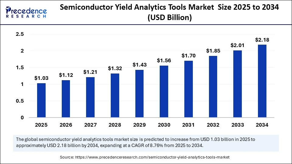
The global semiconductor yield analytics tools market is on a robust growth trajectory, forecasted to grow from USD 1.03 billion in 2025 to approximately USD 2.18 billion by 2034, reflecting a compound annual growth rate (CAGR) of 8.76%. This rise is driven by the increasing complexity in semiconductor manufacturing, the integration of AI and machine learning for real-time defect detection, and a global surge in demand for high-performance chips.
What is Driving the Growth of the Semiconductor Yield Analytics Market?
Semiconductor manufacturing faces heightened challenges as advanced nodes become smaller and more complex, requiring sophisticated analytics tools for optimizing yields. Traditional process controls can no longer fully address defects and variabilities in wafer fabrication. The integration of AI and machine learning enables fabs to detect defects earlier, analyze hidden patterns, and optimize processes dynamically, thereby reducing downtime, lowering waste, and accelerating product time-to-market.
Semiconductor Yield Analytics Tools Market Quick Insights
-
The market size reached USD 0.94 billion in 2024 and is expected to grow at a CAGR of 8.76% from 2025 to 2034.
-
Asia Pacific dominates with a market size of USD 433.66 million in 2024, expected to exceed USD 1 billion by 2034.
-
North America is the fastest-growing region, driven by new fabrication projects and investment in secure cloud platforms and AI-integrated yield solutions.
-
Leading companies innovating in this market include Synopsys, Applied Materials, ASML Holding, KLA Corporation, HORIBA, Bruker, Merck, and Tokyo Ohka Kogyo.
-
Yield management software, particularly defect analysis software, holds around 40% revenue share in 2024.
Semiconductor Yield Analytics Tools Market Revenue Breakdown (USD Billion)
| Year | Market Size (USD Billion) |
|---|---|
| 2024 | 0.94 |
| 2025 | 1.03 |
| 2034 | 2.18 |
AI and machine learning have become pivotal in optimizing semiconductor yield analytics. These technologies empower fabs to perform real-time defect isolation, predictive maintenance, and closed-loop process optimization, which traditional methods could not achieve effectively. AI-enabled tools analyze vast datasets from wafer fabrication and testing to identify subtle trends and root causes of yield loss, helping manufacturers implement proactive corrective measures.
For example, Synopsys introduced an AI-assisted design tool co-developed with Microsoft Azure OpenAI that enhances yield optimization by integrating design insights with manufacturing analytics. This not only speeds up defect identification but also supports predictive adjustments in production. The role of AI is expanding beyond mere defect detection, into holistic production enhancement by fusing data from fabrication, assembly, and testing phases.
What Are the Key Growth Factors Fueling This Market?
-
Rising complexity of semiconductor nodes beyond 7nm, requiring advanced analytics to maintain yield rates.
-
Increasing adoption of EUV lithography and 3D packaging technologies, prompting the need for sophisticated defect pattern analysis.
-
Growing governmental support and investments in semiconductor manufacturing infrastructure globally.
-
Demand for high-reliability chips for automotive, consumer electronics, and high-performance computing sectors.
-
Expansion of fabless companies leveraging yield analytics through partnerships with foundries.
What Opportunities and Trends Are Shaping the Market?
-
Can contamination control and real-time analytics help reduce wafer yield loss? Contamination impacts around 50% of wafer yields, intensifying the demand for tools that monitor and correlate contamination sources with defect patterns to prevent waste.
-
Could the integration of Advanced Process Control (APC) with yield analytics create breakthrough production efficiencies? Real-time monitoring and adjustments enabled by APC combined with analytics are opening new avenues for minimizing scrap and maximizing throughput, especially at sub-3nm nodes.
Semiconductor Yield Analytics Tools Market Regional and Segmentation Analysis: Who Leads and Who Follows?
-
Asia Pacific leads the market, thanks to its vast manufacturing capacity, governmental backing, and rapid adoption of advanced nodes and packaging technologies. Taiwan, in particular, stands out with its advanced foundry ecosystem and collaborative innovation.
-
North America is the fastest-growing region propelled by new fab projects, cloud-based analytics adoption, and government incentives aimed at boosting local semiconductor manufacturing capabilities.
-
Europe, Latin America, and Middle East & Africa are developing markets with emerging investment and increasing focus on wafer fab improvements.
Semiconductor Yield Analytics Tools Market segmentation highlights:
| Segment | Dominant/Sub-segment |
|---|---|
| Tool Type | Yield management tools, especially defect analysis software (40% revenue share in 2024) |
| Component | Software segment dominating, led by yield enhancement and predictive modeling software |
| Application | Wafer fabrication largest segment; process optimization fastest growing |
| End User | Semiconductor foundries largest segment; fabless companies growing fastest |
What Are the Recent Breakthroughs from Top Companies?
-
Synopsys introduced AI-assisted Copilot with Microsoft Azure OpenAI to enhance design and yield optimization.
-
TSMC increased investments in advanced metrology and process monitoring to improve yields for next-gen logic chips (May 2024).
-
Applied Materials launched SEMVision™ H20 defect review system using eBeam and smart tech for nanoscale defect analysis (February 2025).
Other key players driving innovations include ASML Holding, KLA Corporation, HORIBA, Bruker, Merck, Tokyo Ohka Kogyo, ASE Technology, Amkor Technology, and Hitachi High-Tech.
What Challenges and Cost Pressures Does the Market Face?
-
Increasing complexity at sub-5nm nodes causing unpredictable yield losses hard to tackle through analytics alone.
-
Significant financial impact due to stochastic patterning errors and contamination-related defects.
-
High R&D expenditure for integrating AI/ML with fabrication and packaging processes.
-
Balancing cost-efficiency with the need for continuous innovation in yield improvement tools.
Case Study: Proactive Contamination Control Using Yield Analytics at a Leading Fab
A top-tier semiconductor manufacturer implemented an AI-empowered yield analytics platform to trace contamination sources in real time. The system correlated defect patterns with contamination events, allowing process engineers to take immediate corrective actions. This new approach reduced wafer scrap rates by 15% within the first year, improved first-pass yield by 8%, and cut downtime through predictive maintenance, illustrating the transformative impact of contamination control integrated with advanced analytics.
Read Also: Quantum Cryptography Market
You can place an order or ask any questions, please feel free to contact us at sales@precedenceresearch.com |+1 804 441 9344