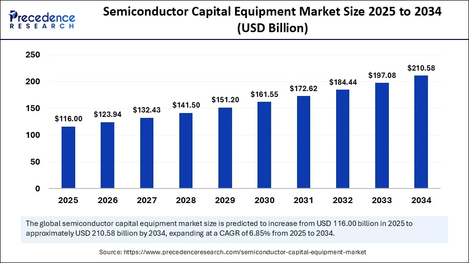
The global semiconductor capital equipment market, valued at USD 108.56 billion in 2024, is projected to expand to USD 210.58 billion by 2034, registering a CAGR of 6.85% from 2025 through 2034. This thriving outlook is propelled by surging investments in AI and high‑performance chips, escalating global foundry expansion, and government incentives to boost semiconductor sovereignty.
Semiconductor Capital Equipment Market Quick Insights
-
In 2024, the market stood at USD 108.56 billion, nearly doubling to USD 210.58 billion by 2034.
-
Asia‑Pacific leads adoption of capital‑intensive tools, with highest regional demand.
-
Top equipment vendors include ASML, Applied Materials, Lam Research, KLA Corporation, and Tokyo Electron.
-
Between 2025–2027, global chip‑making equipment spend is forecast at USD 400 billion, with USD 123 billion expected in 2025 alone.
-
Photolithography, etching, deposition, and inspection/metrology remain core high‑investment categories.
-
The foundry segment continues to dominate end‑user equipment consumption.
Semiconductor Capital Equipment Market Revenue Breakdown
| Year | Market Value (USD Billion) |
|---|---|
| 2024 | 108.56 |
| 2034 | 210.58 |
| CAGR (2025–2034) | 6.85% |
AI is no longer just a chip consumer—it’s reshaping the capital equipment market itself. Machine learning systems embedded into photolithography and etch tools are providing predictive maintenance, yield optimization, and real‑time process control—vital for sub‑5 nm and 3D packaging production.
Meanwhile, AI‑powered process simulation and automation are compressing development cycles, allowing foundries to push advanced nodes faster. As chip designs grow more complex, equipment must become adaptive—and AI is the nerve center of that transformation.
Read Also: Semiconductor Foundry Market
Semiconductor Capital Equipment Market Scope
| Report Coverage | Details |
| Market Size by 2034 | USD 210.58 Billion |
| Market Size in 2025 | USD 116.00 Billion |
| Market Size in 2024 | USD 108.56 Billion |
| Market Growth Rate from 2025 to 2034 | CAGR of 6.85% |
| Dominating Region | Asia Pacific |
| Fastest Growing Region | North America |
| Base Year | 2024 |
| Forecast Period | 2025 to 2034 |
| Segments Covered | Equipment Type, Technology Node, Wafer Size, Application, End-Use Industry, Distribution Channel, and Region |
| Regions Covered | North America, Europe, Asia-Pacific, Latin America, and Middle East & Africa |
Key Market Growth Drivers
-
AI‑ and data‑center‑grade chip production is rapidly scaling, necessitating cutting‑edge fabrication equipment.
-
Foundry expansion in Asia-Pacific, Europe, and North America is prompting fab capex and equipment order spikes.
-
Supportive government policies, like the U.S. CHIPS Act and EU Chips Act, are underwriting domestic equipment procurement.
-
Shift to advanced packaging (3D/2.5D, chiplets) demands new assembly, inspection, and bonding tools.
What’s Driving Opportunities and Market Trends?
How is 3D packaging reshaping capital equipment demand?
As chiplets and hybrid bonding gain traction, inspection and assembly tools for advanced packaging are becoming must-have technologies.
What impact does sustainability have on next-gen equipment?
Manufacturers are increasingly seeking low-emission gas tools and lightweight consumables—driving eco‑friendly design in capital equipment.
Expert Insight
“This market is at the intersection of national strategy and advanced manufacturing. The push for chip sovereignty, together with AI and 3D packaging, guarantees sustained demand for lithography, inspection, and wafer processing tools,” says Dr. Priya Shah, Principal Consultant, Semiconductor Equipment, Precedence Research.
Semiconductor Capital Equipment Market Regional Analysis
Asia-Pacific
The region dominates the market and is home to leading foundry hubs like Taiwan, South Korea, China, and Japan. These countries continue to lead global equipment spending, driven by TSMC, Samsung, and SMIC. Their focus on 3 nm and below node development, combined with domestic policy incentives, solidifies their leadership.
North America
Driven by initiatives under the CHIPS Act, North America is reinvesting heavily in local semiconductor manufacturing. Intel, Micron, and GlobalFoundries are expanding fab capacities, driving demand for advanced lithography, deposition, and metrology equipment.
Europe
Europe is rebuilding its semiconductor ecosystem with a focus on specialty chips, automotive semiconductors, and photonics. National funding and the EU Chips Act are enabling the region to invest in cleanroom fabs, particularly for power electronics and RF chips.
Semiconductor Capital Equipment Market Segmentation Overview
By Equipment Type
-
Photolithography Equipment – Crucial for pattern transfer; leading in value share.
-
Deposition Equipment – CVD, PVD, and ALD systems for layer building.
-
Etching Equipment – Used to shape wafer materials with high precision.
-
Cleaning Equipment – Ensures wafer surfaces are defect-free.
-
Inspection and Metrology – For quality control at nanoscale levels.
By Application
-
Front-End Equipment – Focused on wafer processing and transistor formation.
-
Back-End Equipment – Used for packaging, bonding, and testing.
By Chip Dimension
-
2D ICs
-
2.5D ICs
-
3D ICs – Emerging as a high-growth area due to 3D integration.
By Fab Facility
-
Foundries – Largest consumers due to outsourced chip production.
-
Integrated Device Manufacturers (IDMs) – In-house chip production with custom equipment needs.
Latest Company Breakthroughs
Industry leaders are fueling the market with groundbreaking advancements:
-
ASML – Continues to lead EUV lithography with new high-NA tools.
-
Applied Materials – Introduces advanced materials engineering solutions.
-
Tokyo Electron – Expands next-gen etching and deposition tool capabilities.
-
Lam Research – Pioneering dry etch technologies for 3 nm and below.
-
KLA Corporation – Strengthens AI-powered inspection and metrology offerings.
Challenges Impacting Market Expansion
-
Capital intensity – High upfront costs limit access for smaller fabs.
-
Supply chain risks – Material and part shortages disrupt equipment delivery.
-
Talent gaps – Shortage of skilled semiconductor engineers and tool developers.
-
Technology complexity – Sub-5 nm and 3D ICs require hyper-precise equipment calibration.
Real-World Snapshot: Foundry Capex Boom in Asia-Pacific
The semiconductor race is being led by Asia-Pacific. Taiwan’s TSMC and South Korea’s Samsung have aggressively expanded production capabilities, placing bulk orders for EUV, etch, and wafer cleaning systems. China’s domestic push has added further momentum, reinforcing the region’s role as the epicenter of equipment spending.
Get the Full Report Today
Explore detailed segment analysis, market forecasts, and company profiles in our comprehensive market report.
👉 Download Sample Report: https://www.precedenceresearch.com/sample/6474
Schedule a Strategy Call with our semiconductor insights team today: sales@precedenceresearch.com