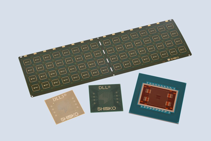
Background
The semiconductor industry has rapidly shifted from traditional packaging methods (like wire bonding and flip-chip) to advanced forms such as 2.5D/3D integration, fan-out wafer-level packaging, and heterogeneous integration. While much attention is given to silicon, interposers, and interconnects, the “soft side” of packaging — polymer-based materials like underfills, die attach adhesives, encapsulants, mold compounds, and thermal interface materials — plays an equally critical role.
These materials dictate mechanical stability, thermal performance, and reliability of the package. However, their behavior is far harder to predict and standardize than hard materials (like silicon or copper).
The Initiative
In 2025, a consortium of NIST (National Institute of Standards and Technology), NC State University, NREL (National Renewable Energy Laboratory), Intel, and other partners launched a joint initiative to map out the critical material and measurement challenges in packaging polymers.
Key Challenges Identified
-
Long Material Adoption Cycles
-
Unlike silicon innovations that may commercialize in 5–7 years, polymer materials often take 10–25 years to move from lab to high-volume production.
-
This is due to stringent reliability requirements, lack of predictive models, and inconsistent performance across suppliers.
-
-
Lack of Standardized Reference Materials
-
The industry has no common “yardstick” for characterizing soft materials.
-
For example, two labs may measure cure shrinkage or glass transition temperature of an underfill differently, leading to poor reproducibility.
-
-
Measurement Gaps
-
Critical properties such as residual stress, cure kinetics, warpage, and adhesion strength at interfaces are poorly measured with current tools.
-
Advanced packaging creates multi-scale stress environments (from nanoscale bumps to large organic substrates) that polymers must withstand, but testing is not standardized.
-
-
Process–Structure–Property Disconnect
-
The behavior of packaging polymers is highly dependent on processing conditions (curing, pressure, temperature cycles).
-
Today, there is a weak link between how materials are formulated, how they are processed, and how they ultimately perform in the package.
-
-
Data & Modeling Limitations
-
Multiphysics modeling of packaging reliability (thermal, mechanical, electrical) often relies on oversimplified polymer data.
-
Without accurate inputs, simulations can’t fully capture delamination risks, void formation, or fatigue failures.
-
Industry Impact
-
Reliability Risks: With AI accelerators, HPC chips, and EV power modules generating higher heat, weak links in polymer packaging can cause catastrophic field failures.
-
Innovation Bottleneck: The slow adoption cycle means new packaging architectures (chiplets, fan-outs, glass interposers) are delayed by limitations in “soft” materials.
-
Economic Costs: Failures traced to packaging polymers can cost millions in recalls or warranty claims.
Proposed Solutions & Recommendations
-
Cross-Industry Consortia
-
Establish partnerships (similar to SEMATECH for silicon) dedicated to packaging polymers.
-
Jointly fund shared reference materials and testing protocols.
-
-
Metrology Development
-
Develop new measurement methods for:
-
Residual stress at micro/nano scale
-
Real-time monitoring of curing and adhesion
-
Long-term degradation under cyclic thermal/mechanical loading
-
-
-
Standardization Efforts
-
NIST and partners advocate creating standard reference materials for polymer testing, enabling labs worldwide to compare results consistently.
-
-
Materials Informatics
-
Use AI/ML + big materials datasets to predict how formulation changes affect properties and reliability.
-
This shortens the 10–25 year cycle for new materials to reach industry.
-
-
Closer Academia–Industry Collaboration
-
Encourage “precompetitive research” where companies like Intel, TSMC, Amkor, and OSATs share data with universities to accelerate breakthroughs.
-
Takeaways
-
This case study underlines that semiconductor packaging innovation is not only about silicon or copper — polymers matter just as much.
-
Without better measurement science, standardization, and predictive modeling, the industry risks bottlenecks that slow the deployment of chiplets, AI chips, EV power modules, and photonics.
-
The NIST-led initiative is a step toward creating a materials measurement ecosystem where advanced packaging can scale reliably, sustainably, and faster.

- ESG Software Market 2025: Comprehensive Company Ecosystem and Revenue Overview - May 20, 2026
- ESG Software Market Surges Toward USD 31.96 Billion by 2035 as AI-Powered Compliance and Sustainability Reporting Transform Global Enterprises - May 20, 2026
- Hematopoietic Stem Cell Transplantation Market Surges Toward USD 24.32 Billion by 2035 as Precision Medicine and AI Reshape Blood Cancer Treatment - May 20, 2026